Search
S3: Evolution of high-resolution ADC efficiency over the years
Title:Role of Dielectrics from Field Effect Transistors to Nan-Systems
Location: Meeting Room 1, 3rd Floor, Crowne Plaza Kunming City Centre
Time: 17:15-18:00, Oct. 22, 2025, Wednesday
Speaker: Prof. Maurits Ortmanns (University of Ulm, Germany)
Abstract: In today’s increasingly digitally connected world, the analog-digital converters remain a unique key enabling component. This presentation begins with a brief look at the era preceding the advent of integrated ADCs, followed by an overview of architectural innovations and performance developments spanning nearly 50 years since their introduction. The discussion emphasizes the most impactful advancements while also reflecting on "the good, the bad and the ugly" side of commonly used figures of merit. Finally, several recent design examples are presented to illustrate how performance improvements of high-resolution ADCs are still achieved.
Bio:
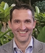 Prof. Maurits Ortmanns received his Dipl.-Ing. in Electrical Engineering from the University of Saarland, Saarbrücken, Germany, in 1999 and his Dr.-Ing. from the University of Freiburg, Germany, in 2004, both with highest distinction.
In 1997 and 1998, he worked as an engineering intern at the Forschungszentrum Karlsruhe, Germany, and at EXAR, Inc., Fremont, CA, in the field of microsensors. In 1999, he joined the Institute of Microelectronics at Saarland University as a research assistant. In 2001, he moved to the Institute of Microsystems Technology at the University of Freiburg, where he worked on his Ph.D. thesis in the area of continuous-time sigma-delta modulator design until 2004.
From 2004 to 2005, he worked at sci-worx GmbH, Hannover, Germany, where he worked on mixed-signal and analog circuits for biomedical implants, low-voltage and low-power applications, and high-speed circuits. In early 2006, Dr. Ortmanns joined the HSG-IMIT, Villingen-Schwenningen, Germany, and was also a visiting lecturer at the University of Freiburg, Germany. In May 2006, he was appointed junior professor for integrated interface circuits at the Institute of Microsystems Technology in Freiburg.
Since 2008, Prof. Ortmanns is a full professor at the University of Ulm, Germany, where he heads the Institute of Microelectronics. Prof. Ortmanns' main research interests include mixed-signal integrated circuit design, self-correcting and reconfigurable analog circuits, with special emphasis on data converters and implantable electronics.
Prof. Ortmanns received the VDI and VDE award in 1999, the best student paper awards at MWSCAS 2009, SampTA 2011, BioCAS 2019, the ITG Publication Award 2015, the best demo awards at ICECS 2016 and SENSORS 2017, the best paper ward at BioCAS 2019, the ESSCIRC best paper award in 2023, and the faculty teaching awards in 2012, 2015, and 2019.
He has been a program committee member of ESSIRC, DATE, ICECS, and ECCTD, an associate editor of IEEE Transactions of Circuits and Systems I and II, and an associate and guest editor of the IEEE Journal Solid State Circuits. Prof. Ortmanns was a member of the Technical Program and Executive Committee of the IEEE International Solid-State Circuits Conference (ISSCC) from 2012 to 2016, the European Regional Chair of ISSCC 2015, and he was the Analog Subcom Chair of ISSCC from 2021 to 2023. He is the TPC Chair of ESSERC in 2025. He was a Distinguished Lecturer for SSCS from 2018-2019 and from 2024-2025. He is a member of the SSCS AdCom for 2025-2027. He is also a founding member of the SSCD. He holds numerous patents, is the author of the book "Continuous-Time Sigma-Delta A/D Conversion" and several other book chapters, and has contributed about 350 IEEE journal and conference papers
IEEE Electron Devices Society is celebrating 100 years of the Field Effect Transistor (FET) in 2025. The first Canadian patent was filed by Julius Lilienfeld on 22 October 1925. During the past century there were phenomenal developments and innovations of the FET that contributed to many applications including computing and communications. The contribution of dielectrics to FET’s development is highly significant. Historically SiO2 was the main driver of MOSFETs as the transistor’s gate dielectric. Once the thickness of SiO2 reached the onset of direct tunneling region (<1.5 nm) HfO2-based high-k insulators were introduced to suppress the direct-tunneling leakage current. The transistor has transformed from a planar device to a three-dimensional device to a gate all around device. Several applications of high-k dielectrics have emerged incuding ferroelectric FETs and resistive random-access memory (RRAM) devices that are being investigated for possible implementation in systems with artificial intelligence hardware. The electrical performance in these devices depends on the dielectric deposition process, precise selection of deposition parameters, pre-deposition surface treatments and subsequent thermal budget. The talk will outline the role of dielectrics from FETs to modern nanoelectronics devices and systems.








 loading......